Quantum nano-emitters coupled to nanofibers
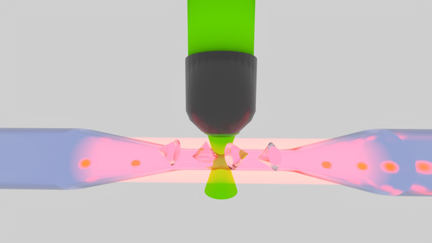
To collect but also to probe nano-emitters, we deposit them on our tapered optical nanofiber and collect their emission in a single guided mode.
Single nanocrystal quantum dot coupled to a nanofiber
Recently we have developed a technique to study the coupling of high-quality non-blinking CdSe–CdS nanorods with a tapered optical nanofiber (TONF). The high collection efficiency of the TONF method, associated with the advantages of dot-in-rod nanocrystals (room-temperature fluorescence, non-blinking, polarization control), are key ingredients to realize a high-quality single-photon source. The main objective of this experiment is to investigate original approaches for coupling optical fibers to solid-state quantum emitters (semiconductor nanocrystals).
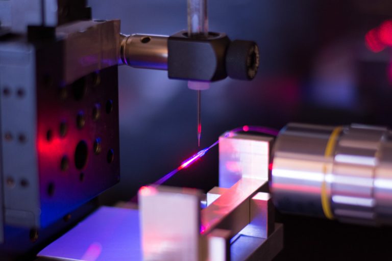
Method. A CdSe–CdS nanorod is deposited on the fiber using a nano-positioning system with a lateral precision of 0.1 μm. An excitation laser (cw or pulsed laser diode) is then focused using an inverted microscope on the nanorod, and fluorescence emission is collected at both ends of the fiber and measured with avalanche photodiodes. The detection setup can be modified to measure the g⁽²⁾ correlation function and verify that the nanorod is indeed a single quantum emitter.
Preliminary results
Preliminary results (light collection through the fiber, g⁽²⁾ measurements) have been obtained recently, and we have managed to produce a TONF with a waist of 300 nm and a transmission greater than 98%.
Moreover, direct photoluminescence signal has been collected through the nanofiber after excitation in free space at 405 nm, with up to 23% efficiency. With various upgrades we are currently implementing, this device is expected to be the first room-temperature single-photon source with collection efficiency near unity.
Deterministic coupling of a single quantum emitter in nanophotonic structures
For most of our applications, we need nanometric resolution on the deposition of the quantum emitters in our photonic nanostructure. To do so, we are using a fluorescent scanning nanoprobe developed at Institut Langevin in the group of Yannick De Wilde and Valentina Krachmalnicoff. With this technique it is possible to graft fluorescent objects sized between 20 and 100 nm on the apex of an AFM tip (tapered silica fiber).
Method
The established grafting procedure is the following:
- first, the emitters are spread on a glass cover-slide, in order to reach an average distance of about 10 μm between two nearby emitters;
- second, the AFM tip is approached to the surface;
- third, the AFM tip scans the region where the emitter to be grafted is located. When the extremity of the AFM tip coincides exactly with the position of the emitter, the emitter sticks to the tip. The fluorescent tip is then retracted and moved to the sample of interest.
During each stage of this procedure, the tip and the emitter are monitored using an EMCCD camera which registers the fluorescence signal in wide field. The signature of the success of the procedure is the disappearance of the grafted emitter from the field of view of the camera when the AFM tip is lifted by a few microns above the glass cover-slide. Adhesion between the emitter and the tip is so good that the emitter can remain grafted on the tip for several hours. As the grafting procedure is very well mastered, we believe it will be possible to have perfect control of the complementary procedure allowing the release of the emitter on the sample in a deterministic way. A thorough study of the orientation of the dipole moment of the emitter, when grafted on the tip and when deposited on the sample, will be done.
Credit: Valentina Krachmalnicoff (Institut Langevin) for the emitter-grafting technique.
Emitter release
Finally, different strategies can be used to release the emitter on the TONF. One possibility is to strongly shake the tip by increasing the oscillation amplitude of the tuning fork; this technique works but is probably not the most precise. A second possibility is to approach the fluorescent AFM tip to the sample and push it against the substrate in order to increase the adhesion between the sample and the emitter. Following the same idea, we shall try to scratch the functionalized tip on the sample until the emitter is wiped away.