Nanophotonics structures with optical nanofibers
One of the most commonly faced problems with semiconductor single-photon sources is implementing fluorescence collection with high efficiency. We are specialized in tapered optical nanofiber engineering to collect single-photon emission.

Nano-waveguide fabrication with tapered fibers
Tapered optical nanofibers
One of the key points to collect fluorescence with high efficiency is to achieve strong confinement of the field using photonic or plasmonic nanostructures. There have been spectacular recent successes in this field, brought by the merging of nanofiber optical cavity systems with cold neutral atoms: it has been demonstrated that 28% of a single atom’s fluorescence can be channeled into the guided mode of a sub-wavelength tapered optical nanofiber (TONF).
We have built a tapering bench based on commercial optical fibers, elongated and tapered down to 300 nm diameter. Careful SEM characterizations have demonstrated good agreement with our simulated pulling profile.
Nanostructures on Nanofibers
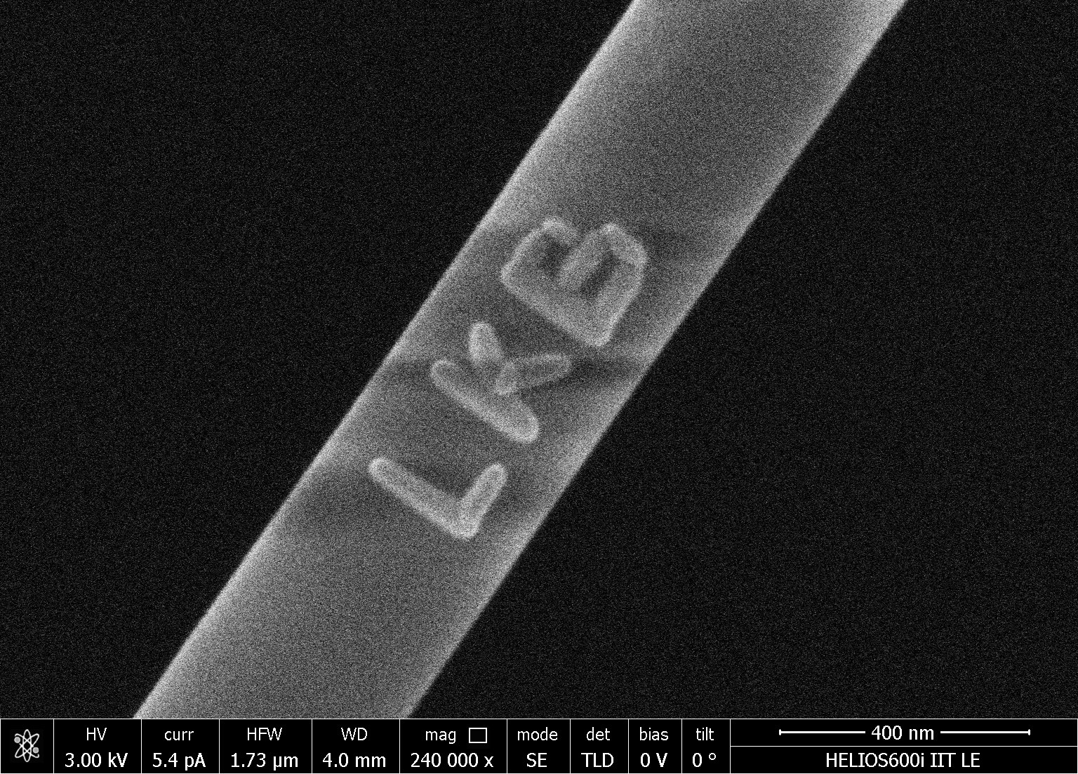
In collaboration with our partner at Istituto Italiano di Tecnologia in Lecce, we use Blurred Electron Beam-Induced Deposition (BEBID) to grow nanostructures directly on the fragile waist of tapered optical nanofibers. By deliberately defocusing the electron beam, we reduce mechanical stress on the suspended fiber while precisely controlling the structures’ position, geometry, and composition. We demonstrated the fabrication of platinum-based nanopillars and nanoantennas with sub-20-nm positioning accuracy; by selecting different precursors, the technique can also be adapted to grow a variety of metallic or dielectric structures.
Hybrid photonic-plasmonic nanostructures
In order to strengthen the coupling between the emitters and a tapered optical nanofiber, we are investigating the effect of plasmonic enhancement. The presence of a plasmonic structure at the surface of the nanofiber can result in an increase of the local density of optical states (LDOS), and therefore in an increase of the probability of coupling between the emitter and the dielectric structure. However, due to Ohmic losses, the propagation length of a surface plasmon is much smaller than the propagation length of photons inside an optical fiber.
Therefore, in order to keep the advantages of both dielectric and plasmonic environments, it is interesting to limit the plasmon–emitter interaction region to a small size, devoted to enhancing the decay rate of the emitter into the guided mode, while using the guided mode of the fiber as a long-range energy transfer vector. We are working to design and optimize these nanostructures by numerical simulations using commercial FDTD software.
Structures under study are plasmonic nanoantennas (such as a gold Yagi–Uda antenna grown by M. Mivelle on a nanofiber) and plasmonic gratings. Hot spots of the hybrid mode present in the proximity of the plasmonic structures should ensure a coupling of the fluorescence of emitters with the nanostructure.